
Semiconductor Packaging Inspection
Terahertz technology enables rapid high accuracy fault isolation in advanced semiconductor packages.
Advanced Packaging fault isolation case studies and advancement of Electro Optical Terahertz Pulse Reflectometry (EOTPR)
EOTPR is a well-established non-destructive fault isolation tool for advanced IC devices. These examples will show how EOTPR has been implemented to investigate a wide range of advanced package types, including 2.5D and 3D packages, wafer level fanout packages, and microelectromechanical (MEMs) devices. Further, we present the recent improvements to the EOTPR instrument and the results from a novel modelling approach that has the potential of vastly speeding up the fault localisation analysis.
Electro-Optical Terahertz Pulse Reflectometry (EOTPR) is an implementation of the time domain reflectometry (TDR) technique at terahertz frequencies, proven to enhance fault isolation accuracy to better than 10 µm. As in conventional TDR, the fault detection accuracy of EOTPR is a function of the rise time of the incident pulse, the time-based jitter, and signal-to-noise ratio (SNR). The EOTPR instrument generates a terahertz pulse using an ultrafast laser and a pair of photoconductive switches for signal generation and detection, resulting in a system with (i) high measurement bandwidth, (ii) low time-base jitter, and (iii) a high time-base resolution.
Compared to conventional TDR, EOTPR generates signals with faster rise time, has greater SNR, and a much-reduced time base jitter; system properties that offer the potential for a significantly increased distance-to-defect accuracy.A schematic diagram of the EOTPR system is shown below.
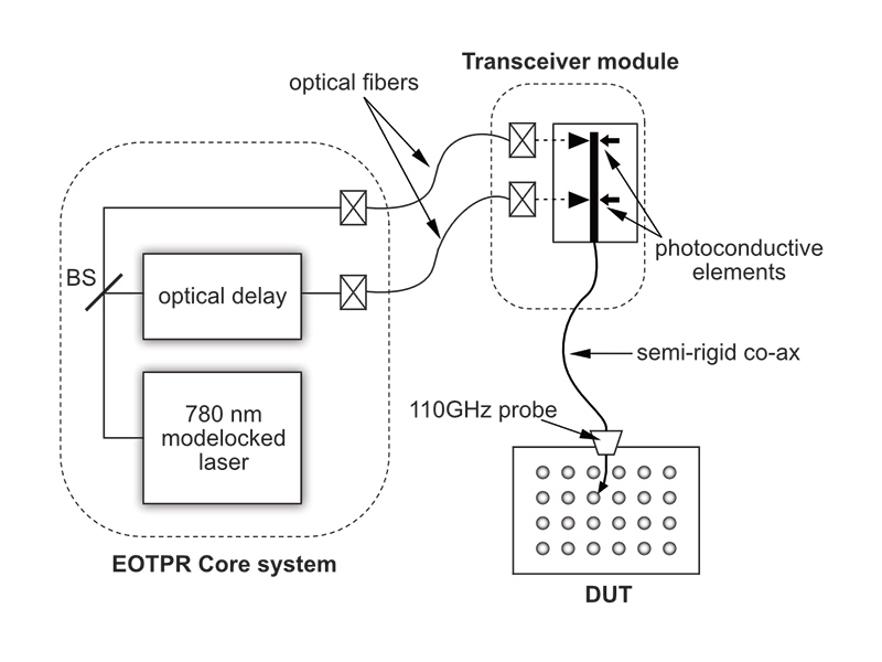
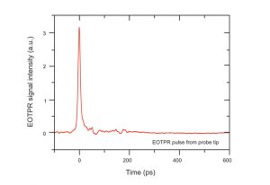
During operation, pulses are launched into a device-under-test (DUT) via a high frequency circuit probe. Portions of the pulse are reflected as it encounters changes in impedance, such as dead opens, resistive opens, and short circuit defects, within the IC. These reflections are measured by the detector photoconductive switch and are recorded as a function of time, resulting in the EOTPR waveform. An example waveform for an open high frequency probe is shown below.
As EOTPR utilises an impulse response rather than the step response of conventional TDR, high and low impedance discontinuities in a DUT result in positive peaks and negative troughs, respectively, in the measured waveform. The magnitude of these features indicates the size of the impedance change encountered by the pulse and their arrival time gives the location of the fault. EOTPR is, by necessity, a comparative technique; to understand whether a waveform feature arises from a fault in the DUT, it is essential to compare the waveform from a known good device (KGD).
To localise a fault within the DUT the time-domain waveform can be readily converted into the distance-domain. This can be accurately achieved by measuring reference devices that have impedance features, such as opens, at known locations. The effective dielectric constant of the DUT can be determined by measuring the time required for the EOTPR signal to travel between reference features or known locations, which is then used to convert the EOTPR waveform from time to distance.
EOTPR is now a well-established technique in failure analysis workflows and has been used to interrogate a wide range of different device architectures. Examples below show how EOTPR can be used to accurately localise faults in advanced IC packages.
Results and Discussion
2.5D Architectures
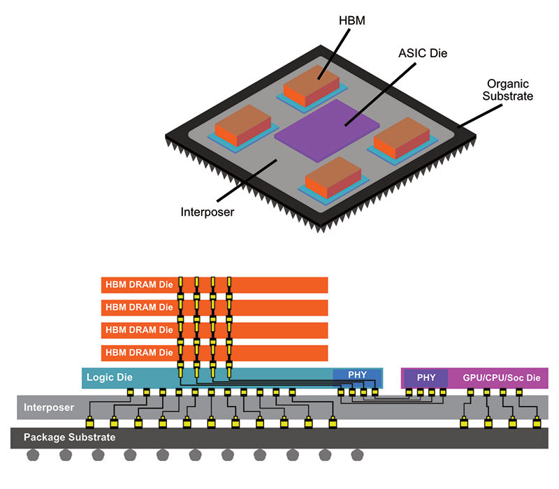
The image below shows a schematic of a 2.5D package consisting of an application-specific IC (ASIC) die and high bandwidth memory devices assembled onto an interposer, and subsequently mounted on an organic substrate. In such devices, defects such as cracks and delamination can occur at the interfaces due to stress induced during the solder reflow and under-fill curing cycles that are used in the manufacturing environment.
In this example, a curve trace performed whilst biasing a signal pin with respect to the ground pin identified an open failure. TDR measurements suggested the open failure lay between the substrate and interposer terminations but could not accurately identify the location. 2D Real Time X-ray and acoustic imaging also could not reveal any anomalies at the associated signal pin interconnects, µbump and C4 interface.

EOTPR was subsequently used to obtain a more accurate defect location. The graph below shows the waveforms obtained for the failed unit (red trace), for a KGD (green trace), a bare printed circuit board (PCB) substrate that terminates at the C4 bump pad (black trace), and a PCB substrate with interposer, which terminates at the µbump pad (blue curve).
The positive peak in the failed unit waveform, highlighted below, clearly demonstrates the open failure in the device, which is calculated to be 100 µm after the bare substrate termination, corresponding to the top of the C4 bump. Physical failure analysis (PFA) of the device later verified the EOTPR results, revealing that the open fault arose from a passivation layer on the C4 pad, as shown in the inset of below, which is located 105 µm from the bare substrate termination.

Microelectromechanical Devices
The short trace length of MEMs devices can prove challenging for EOTPR investigations, due to their lack of reference features with which to localise the fault. A common workaround is to introduce artificial faults in the reference devices, which can in turn be used to extract the fault location in the failed device.
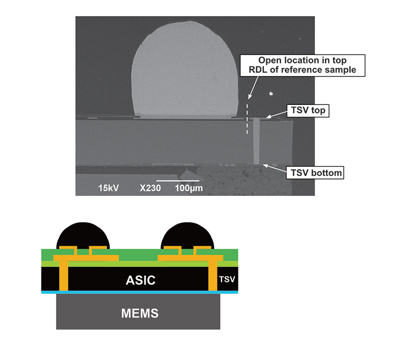
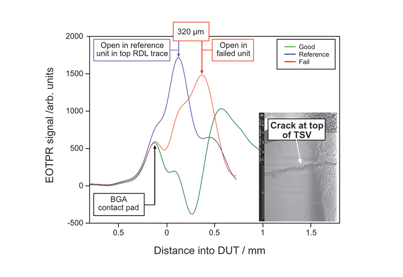
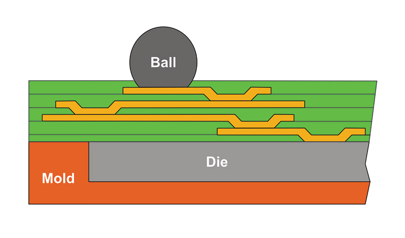
The image above shows a schematic and cross section of a MEMs device used in one such case. The device consists of a MEMs unit mounted onto a substrate, with the electrical connection between the MEMs device and the solder ball made by a through-silicon via (TSV) and a redistribution layer (RDL). The EOTPR waveform obtained for a KGD (green trace), reference device (blue trace), and the failed unit (red trace) are shown below. The reference sample was prepared by cutting the surface signal trace in the RDL of a separate KGD. The approximate location of the cut in shown above. The open peak for the failed sample was calculated to be 320 µm after the cut in the RDL. Later PFA, shown on the inset below, revealed that the fault arose from a crack in the TSV interface, which was separated from the artificial defect by 325 µm.
Wafer-Level Fanout Packages
EOTPR has recently been used to localise faults in the state-of-the-art wafer-level fanout packages, demonstrating the importance of EOTPR at the forefront of package development. The image below shows a schematic of such a device, which consists of non-conventional wafer-level packaging with innovative interconnections, enabling a package-on-package configuration for a memory chip. A custom redistribution device, called Via Frame, allows memory stacking. These components are integrated into an epoxy mold compound on a series of RDLs.
A unit that failed an automated electrical continuity test performed after 1000 temperature cycles within -40℃ to 125℃ range was identified as a suitable candidate for EOTPR investigation. Further curve tracing revealed an open fault on the failed net. Subsequent EOTPR characterisation is presented in the graph below, in which the failed unit’s waveform (red curve) is compared to a KGD (green curve). In addition, the waveform from a reference unit (blue curve) is shown, which has a known open fault located 160 µm from the end of RDL.
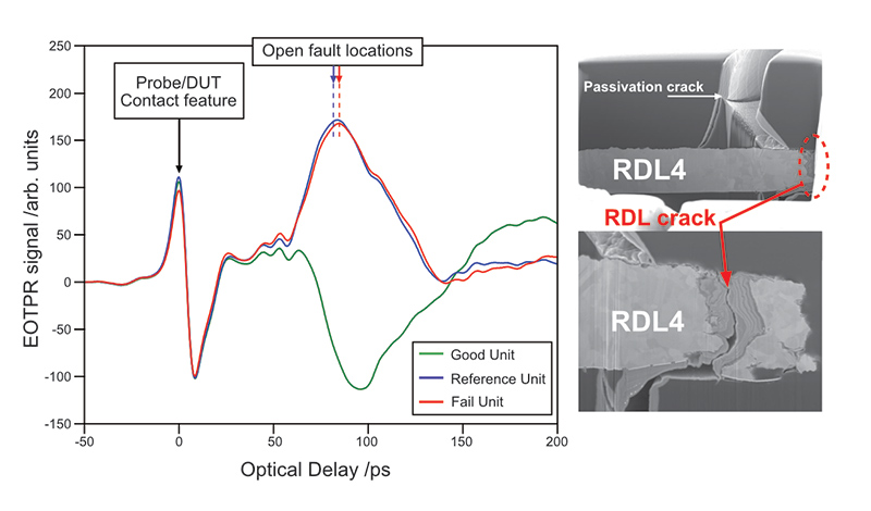
By using the known distance between the reference unit open and the solder ball, the location of the fault in the failed unit was calculated to be 100 µm from the end of the RDL. Confirmation of this location was obtained by PFA, which identified a crack in the copper trace 100 µm from its end, shown above on the right.
3D packages
In this final case study, it was shown that EOTPR can used to identify every key component of a 3D device architecture, and thus is an ideal tool for failure analysis of 3D packages. To isolate each key feature in the EOTPR waveform, a sample device, shown schematically below, was mechanically grinded from top to bottom in steps, with an EOTPR measurement being performed at each step.
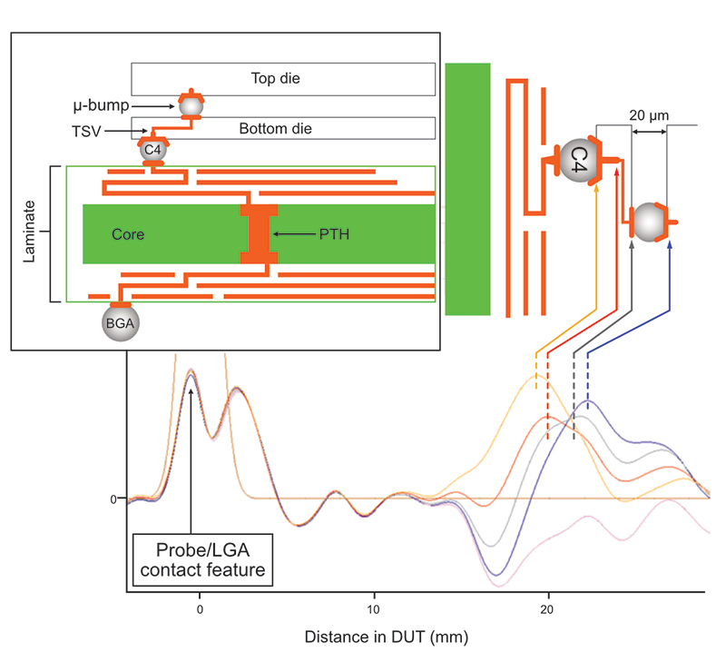
For example, in the first step, the top die was removed, resulting in the measured net being terminated by the exposed µC4 bumps. In the next grinding step, these were in turn removed, moving the termination to the top of the bottom die TSV. In this manner, a complete understanding of the EOTPR waveform can be generated. As individual features of the waveform can be then unambiguously identified, it is possible to scale the obtained waveform and extract accurate distance-to-defect values.